

Categories
Blog Design, Cost & Sourcing

Metal Core PCB Design: Thermal Paths and Heat Sink Integration

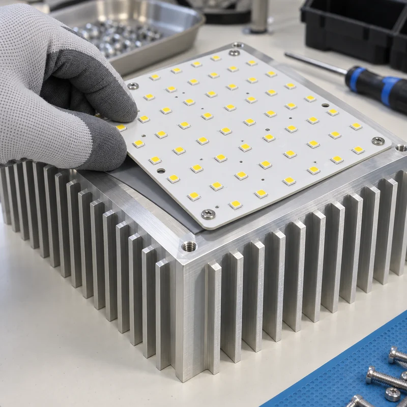
A metal core PCB combines circuitry with a metal heat-spreading structure, usually separated by an electrically insulating dielectric. Its thermal performance depends on the complete path from component to ambient, including dielectric thickness, contact area, interface material, mounting, and heat sink. Naming the metal and board thickness alone does not specify that path.

This guide focuses on the mechanical and thermal handoff between a PCB supplier and an enclosure or heat-sink supplier. MTSPi’s role is mechanical component manufacturing; PCB fabrication, circuit design, and electrical qualification should be confirmed with the appropriate electronics supplier.

Trace Heat Through the Complete Assembly

Begin at the heat-generating component. Heat crosses its package interfaces, copper features, the board construction, any interface material, and finally the heat sink or housing before reaching ambient air or coolant. Spreading and contact effects can matter alongside material conduction.

A metal core can improve heat spreading, but it cannot compensate for every bottleneck elsewhere. If the heat sink has inadequate airflow or the interface contains a gap, changing aluminum to copper may produce much less improvement than expected. Evaluate the assembled thermal network using the actual heat distribution.

Separate Conductivity From Thermal Resistance

Thermal conductivity describes a material property. Thermal resistance describes opposition to heat flow through a particular geometry. In a simplified uniform layer, resistance is thickness divided by conductivity and area. Real board assemblies also include contact, spreading, and geometry effects that this one-dimensional calculation omits.

Henkel’s thermal-interface guidance emphasizes the effects of thickness, area, pressure, and measurement conditions. Request thermal data for the proposed dielectric construction and compare equivalent test methods. A high conductivity value from an unspecified thickness is not enough to predict the component temperature.

Specify the Dielectric and Electrical Isolation Together

The insulating layer must satisfy both heat-flow and electrical requirements. Reducing thickness may help conduction, but electrical breakdown, manufacturing variation, working voltage, creepage, clearance, and product safety requirements still need a qualified review. A datasheet breakdown number should not be substituted for the system’s continuous working-voltage requirement.

Ask for the exact laminate system, dielectric thickness and tolerance, thermal property test method, insulation requirements, and proposed production tests. Confirm whether exposed core edges, mounting holes, screws, and machining burrs could reduce electrical separation in the finished assembly.

Choose the Core and Stackup From the Design

Option Reason to evaluate it Question to settle
Aluminum-based board Heat spreading with relatively low mass Does the full dielectric and mounting design meet the temperature target?
Copper-based construction Applications benefiting from copper’s heat spreading Does the improvement justify mass, cost, and processing changes?
FR4 with an engineered thermal path Routing flexibility and a familiar fabrication route Can vias, copper, and external cooling meet the requirement?
Ceramic substrate Specialized electrical and thermal requirements Are handling, joining, cost, and reliability acceptable?

Do not assign universal layer counts, hole minimums, or dielectric ratings to a core metal. These are construction and supplier capabilities. Obtain a proposed stackup before detailed routing and compare it with the mechanical envelope.

The FR4 specification checklist provides a useful comparison when deciding whether a metal-based route is necessary.

Design Mounting Holes and Contact Surfaces Deliberately

Define whether each hole is plated, insulated, or intended to connect electrically to the core. Through-hole construction can require specific isolation features, and those must be reviewed with the board fabricator. Coordinate fastener head size, washers, conductive debris control, and component keep-outs.

Mounting surfaces should have agreed flatness and condition. A board forced onto an uneven base can bend, lose contact in another area, or stress solder joints. Place screws and supports to achieve the required contact without exceeding permitted board or component loading.

Control the Thermal Interface Instead of Guessing It

Select the interface material with the assembly gap, flatness, contact pressure, temperature, electrical isolation, and rework needs in mind. A thick compliant pad and a thin grease layer solve different assembly problems. Include compression behavior and the permitted installation range in the design review.

For a hypothetical LED module, record board temperature near the heat source, housing temperature, ambient temperature, electrical power, and orientation during testing. A cooler housing is not proof that the LED junction is cooler; the component’s thermal model and measurement method still matter.

Coordinate Heat Sink Geometry With Manufacturing

Fin spacing, airflow access, mounting bosses, threaded holes, surface finish, and tool access all affect the mechanical solution. A larger heat sink may be ineffective if its fins are enclosed without a useful airflow path. Include the final installation condition rather than testing only an open bench arrangement.

Review machined heat-spreader and housing interfaces with MTSPi using the board drawing, thermal-interface area, finish requirements, and critical dimensions. Any coating on the contact face should be considered explicitly in the thermal and electrical design.

Put the Important Requirements on the RFQ

  • Exact core material, thickness, tolerance, and finished stackup.
  • Dielectric system, thickness, thermal data, and electrical-isolation requirements.
  • Copper construction, circuit layer map, holes, and edge details.
  • Finished board envelope, flatness, mounting datum scheme, and keep-outs.
  • Interface material, compression range, fasteners, and assembly sequence.
  • Electrical, thermal, dimensional, and traceability records required for acceptance.

Ask suppliers to identify deviations before production. Treat a different dielectric or interface material as an engineering change even when the outer dimensions remain identical. Keep the PCB and mechanical release revisions linked.

Validate at Operating Conditions

Test representative assemblies at the intended power, duty cycle, ambient conditions, orientation, and cooling state. Include worst-case tolerances where they materially affect contact. Record the stabilization criterion and sensor placement so repeated tests are comparable.

Inspect after relevant thermal or environmental cycling for loose fasteners, interface movement, board distortion, insulation damage, and component or solder-joint problems. Passing a short initial temperature check does not establish lifetime reliability.

Frequently Asked Questions

Is copper always better than aluminum for an MCPCB?

No. Compare the complete construction, heat distribution, mass, cost, and interface. A different bottleneck may dominate the temperature result.

Does a metal core remove the need for a heat sink?

Not necessarily. The core spreads heat; the assembly must still reject that heat to its environment.

Can I change the thermal pad after testing?

Only after reviewing the replacement’s electrical, mechanical, and thermal behavior and repeating the validation needed for the change.

Who reviews the enclosure interface?

The electrical, thermal, PCB, and mechanical teams should agree it together. Send the mechanical requirements through the MTSPi project contact page.
Categories
Blog Design, Cost & Sourcing

FR4 PCB Material: Specifications, Grades, and Enclosure Design

FR4 PCB material is a family of glass-reinforced epoxy laminates, not one interchangeable specification. A useful purchasing package names the laminate or performance class, finished thickness, copper weights, stackup, surface finish, impedance requirements, compliance requirements, and the tests used for acceptance.

This guide explains how to turn “FR4” into a quote-ready material requirement and how that choice affects a machined enclosure. MTSPi manufactures mechanical parts; it does not claim PCB fabrication capability. Confirm laminate, fabrication, and electrical-test requirements with the selected board supplier.

What FR4 Means and What It Does Not

FR4 describes a flame-retardant grade family commonly based on woven glass reinforcement and epoxy resin. It does not identify one resin system, one glass-transition temperature, one dielectric constant, or one approved operating temperature. Two materials described as FR4 can have materially different thermal and electrical properties.

A flame-retardant grade is also not a substitute for a product-level compliance decision. When a flame classification matters, request the laminate manufacturer, exact product designation, relevant UL file, minimum thickness covered, and the board fabricator’s applicable recognition. Do not infer approval from the green color of a finished board.

Use the Datasheet, Not a Generic FR4 Number

Published laminate data show why a generic callout is incomplete. For example, an Isola low-Tg FR4 product lists a 135 C Tg, while a high-Tg FR4 product lists a 180 C Tg. Their decomposition temperature, Z-axis expansion, moisture absorption, dielectric properties, and copper options also differ. These values belong to the named products and test methods; they are not universal FR4 constants.

Property What it describes Why a buyer cares
Tg Transition in the resin system’s mechanical behavior Useful for thermal-process and dimensional-stability review, but not a maximum service-temperature rating
Td Decomposition temperature under a stated test method Helps compare resistance to thermal degradation; it does not replace reflow qualification
Z-axis CTE Expansion through the board thickness Relevant to plated-through-hole and multilayer reliability during thermal cycling
Dk Relative permittivity at a stated frequency and method Affects transmission-line geometry and propagation; use the fabricator’s design value
Df Dielectric loss at a stated frequency and method Matters when insertion loss and high-frequency performance are design constraints
CTI Comparative tracking index under a defined test May influence insulation coordination, but required creepage still depends on the applicable safety standard
Water absorption Moisture uptake under a stated conditioning method Can affect processing, dimensional behavior, and electrical performance

Do not compare isolated values measured by different methods as if they were directly equivalent. Record the test method, frequency, conditioning, and whether a value is typical or guaranteed.

Specify the Thermal Requirement as a Process Window

“High Tg” is useful shorthand only after the assembly process is known. Document the soldering profile, number of expected thermal excursions, board thickness, copper distribution, via construction, and reliability requirement. Tg, Td, time-to-delamination data, and expansion behavior answer different questions.

For lead-free assembly, ask the fabricator to propose a laminate qualified for the agreed stackup and reflow exposure. A high Tg alone does not guarantee low Z-axis expansion, adequate time to delamination, or a robust plated-through-hole construction. If the board will operate hot after assembly, treat continuous operating temperature as a separate application requirement.

Define the Electrical Requirement Before Naming a Substitute

Standard FR4 may be suitable for many digital and low-frequency products, but there is no defensible universal frequency at which it suddenly stops working. Trace length, loss budget, edge rate, impedance tolerance, copper roughness, weave effects, temperature, and moisture all influence the result.

For controlled impedance, provide the target, tolerance, layer reference, and test-coupon requirement. Let the PCB fabricator close the stackup using the actual laminate and copper system, then return the proposed geometry for electrical approval. The HDI stackup and mechanical-integration guide shows how to coordinate that proposal with the enclosure revision.

Move to a characterized low-loss or RF laminate when analysis shows that FR4’s loss or property variation consumes the available margin. Use a metal-core construction when heat spreading dominates and the electrical design supports it. Use a flex construction when the circuit must bend. These are requirement-driven changes, not automatic upgrades.

Make Thickness and Copper Unambiguous

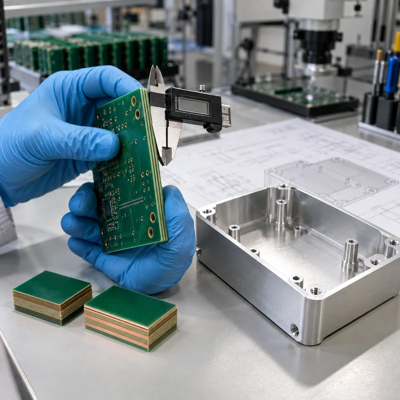
A nominal finished thickness such as 1.6 mm does not define the dielectric structure. State the finished-thickness tolerance, layer count, copper weight by layer, plating assumptions, and approved stackup. If connector fit, card guides, edge contacts, or a compression interface depend on thickness, identify that dimension as a mechanical interface.

Copper should be stated as starting and/or finished copper where relevant. A plated outer layer does not necessarily finish at its starting foil thickness. Heavy copper changes etching, spacing, thermal behavior, and stackup balance, so it belongs in the first quotation package rather than a later note.

Choose Surface Finish From Assembly and Storage Needs

Surface finish affects solderability, pad flatness, storage, rework, and cost. Lead-free HASL, ENIG, OSP, immersion silver, and other options are not interchangeable defaults. Fine-pitch components may need a flatter finish, while storage duration and handling conditions can rule out an otherwise economical option.

Ask the assembly supplier to approve the finish together with the component package and soldering process. If edge contacts, wire bonding, repeated mating, or a specific shelf-life requirement applies, state it explicitly and request the appropriate thickness and inspection evidence.

Coordinate the PCB With the Machined Enclosure

The laminate choice reaches the enclosure through finished thickness, bow and twist, mounting-hole location, connector position, thermal-interface compression, and electrical clearance. A CAD model containing only the bare board outline is not enough for a reliable fit review.

  • Use shared datums for the board holes, enclosure standoffs, and connector openings.
  • Model maximum component height, keep-out zones, screw heads, washers, and cable bend space.
  • Define the acceptable board-thickness range where card guides or edge slots locate the assembly.
  • Review thermal-pad compression without forcing the PCB to become a spring.
  • Keep conductive hardware and machined bosses outside the electrical team’s required clearances.
  • Inspect first-article board-to-housing fit with the populated assembly or a controlled representative fixture.

Send the approved board envelope and interface drawing when discussing machined enclosure features. MTSPi can review the mechanical component, tolerances, material, and inspection scope without representing the PCB fabrication itself.

A Quote-Ready FR4 PCB Specification Checklist

RFQ field Minimum useful content Evidence to request
Laminate Manufacturer/product or approved performance class; Tg/Td/CTE and compliance requirements Datasheet, certificate of conformance, UL file where applicable
Construction Layer count, proposed stackup, finished thickness and tolerance Approved stackup drawing and revision
Copper Per-layer starting/finished requirement as applicable Stackup and cross-section plan
Electrical Impedance targets and tolerances, test coupons, net test requirement Impedance report and electrical-test record
Thermal process Assembly profile, expected cycles, and special operating environment Material suitability confirmation and agreed qualification
Finish Named finish, thickness where relevant, storage/assembly constraints Process certificate or inspection result as required
Mechanical Outline, hole tolerances, bow/twist limit, connector and enclosure interfaces First-article dimensional report
Compliance Applicable IPC class, RoHS/REACH or product-specific requirements Agreed certificates and traceability documents

Include Gerber or ODB++ data, drill files, fabrication drawing, stackup, netlist where required, assembly constraints, and revision identifiers. Ask suppliers to list every proposed deviation instead of silently substituting an available laminate.

When to Stay With FR4 and When to Switch

Stay with a qualified FR4 product when its documented electrical, thermal, mechanical, regulatory, and supply requirements fit the application. Consider a higher-performance laminate when repeated thermal processing or reliability requirements exceed the proposed standard material. Consider low-loss/RF material when simulation and test budgets require tighter and lower dielectric loss. Consider metal-core material for a heat-spreading architecture, polyimide-based flex for controlled bending, or another substrate when the product requirement clearly demands it.

The correct decision is the least exotic material system that passes the complete requirement set with manufacturing margin. A premium laminate cannot repair an incomplete stackup, poor thermal design, or an enclosure that loads the board incorrectly.

Frequently Asked Questions

Is all FR4 the same?

No. FR4 is a grade family. Resin systems, Tg, Td, expansion, moisture absorption, Dk, Df, approvals, and available constructions vary by product.

Does a higher Tg automatically mean a better PCB?

No. It can support certain thermal requirements, but reliability also depends on expansion, decomposition behavior, stackup, via construction, process control, and the actual thermal cycle.

Can I specify only 1.6 mm FR4 and 1 oz copper?

That is enough for a rough budgetary discussion, not a controlled build. Add the exact or approved laminate class, stackup, finished-thickness tolerance, copper definition, surface finish, electrical requirements, and acceptance tests.

At what frequency must FR4 be replaced?

There is no universal cutoff. Use the channel loss budget, trace length, material data at the relevant frequency, impedance tolerance, environment, and validation results to decide.

What should the enclosure supplier receive?

Provide the approved board outline, thickness range, hole and datum scheme, populated height envelope, connector locations, keep-outs, thermal interfaces, and assembly sequence. Use the engineering contact page to submit the mechanical package for review.

Technical reference basis: IPC technical resources on laminate thermal behavior and moisture; published Isola FR4 laminate data; UL material-recognition records; Rogers guidance on high-frequency laminate selection. Values in this article are explanatory only. Use the named product’s current datasheet and the applicable design standard for procurement.

Categories
Blog Design, Cost & Sourcing

HDI PCB Design: Stackup Decisions and Mechanical Integration

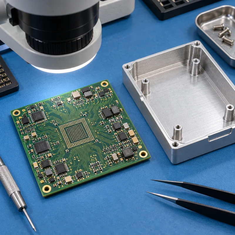
An HDI PCB uses high-density interconnect construction, including microvias and fine routing features, to connect components where conventional routing becomes difficult. It is not defined solely by having many layers. A useful design review connects the electrical stackup to fabrication capability and then checks the assembled board against the enclosure.

This guide addresses engineering handoffs. It does not imply that MTSPi fabricates PCBs or provides a particular electronic assembly certification. Confirm electronic fabrication requirements with the chosen board manufacturer and mechanical component requirements with the machining supplier.

Establish Whether HDI Solves a Real Routing Constraint

Start with the component package, pin map, board outline, routing density, and electrical requirements. A fine-pitch BGA may need a different escape strategy from a larger package with the same logical function. Moving a connector or increasing the board outline may sometimes avoid a costly construction, but those decisions affect the product enclosure and assembly.

Ask the layout engineer to identify the actual bottleneck: insufficient escape channels, excessive layer transitions, limited routing area, or a package geometry that the current via pattern cannot accommodate. “Make it HDI” is not a complete design instruction.

Read the Via Map Alongside the Stackup

Feature Basic role Question to settle
Through via Connects through the board thickness Where does its occupied area restrict routing?
Blind via Connects an outer layer to an internal layer Which layer pair is connected?
Buried via Connects internal layers without reaching an outer surface How is it incorporated into the manufacturing sequence?
Microvia Provides a small, shallow interlayer connection What geometry, filling, and reliability requirements apply?

Do not treat every blind via as a microvia. Supply a layer-pair drawing and define the intended structure. Staggered microvias use offset positions between successive connections; stacked microvias align vertically. They are not interchangeable layout shortcuts. Discuss the specific construction, process capability, and qualification evidence with the fabricator.

Industry HDI design guidance, including Altium’s manufacturing guide, emphasizes that the via structure and manufacturing sequence belong in the design discussion. A visually complete CAD layout does not by itself establish that a shop can manufacture and inspect the intended interconnect reliably.

Select a Manufacturable Build-Up Before Detailed Routing

A notation such as 1+N+1 generally describes one build-up layer on each side of an N-layer core structure. It is a shorthand, not a complete procurement specification. Copper weights, dielectric materials and thicknesses, layer functions, via connections, finished thickness, and impedance requirements still need definition.

Eurocircuits’ published HDI guidance illustrates an important approach: begin with an available build-up and its design rules. Its partial-HDI examples also show that fine routing can be concentrated in part of a construction rather than assumed to require the most complex stack everywhere. Those are supplier-specific offerings, not universal dimensions to copy into an unrelated purchase order.

Agree impedance targets with the actual material and layer structure. Track width alone is insufficient: reference-plane spacing, dielectric properties, copper thickness, and differential-pair spacing all contribute. The board fabricator’s stackup proposal and the designer’s electrical constraints must refer to the same revision.

Check the Mechanical Envelope in Three Dimensions

A smaller board is not automatically a smaller finished product. Connectors, cable bends, component height, thermal hardware, fastening access, and assembly order may control the envelope. A dense board can fit its outline perfectly and still interfere with the enclosure lid.

  • Define a common coordinate origin and mounting-hole datums.
  • Check maximum component height on both sides of the PCB.
  • Include connector mating travel and cable exit space.
  • Keep fasteners and standoffs clear of copper and components as required by the electrical design.
  • Review thermal-pad contact without bending the board through excessive compression.
  • Check access for assembly tools and any required rework.

For an illustrative fit study, export the populated board into the mechanical assembly, add the intended screw heads, and sweep the connector’s mating motion. This can expose a conflict that a bare-board outline check misses. Measure the critical physical interface on first articles instead of relying only on nominal CAD alignment.

Programs using flexible interconnects should also review bend-zone and enclosure-fit considerations. These are separate mechanical constraints, not benefits automatically provided by HDI construction.

Prepare Two Coordinated Manufacturing Packages

The PCB package should contain the agreed fabrication data, layer map, drill and via definitions, stackup, material requirements, finish, impedance targets where applicable, and inspection or test requirements. The mechanical package should contain the enclosure model, drawing, datums, finish, mounting geometry, and approved board envelope.

Use a release table linking both packages to the same assembly revision. If the board thickness changes after quotation, notify the mechanical team: connector height or a retaining feature may depend on that value. Likewise, an enclosure standoff change should not be implemented without checking the populated board.

Discuss machined housing features with MTSPi using the board envelope and interface drawing. Use the project contact page to confirm mechanical scope and required evidence.

Compare Supplier Proposals on Evidence

Request explicit confirmation of the proposed via construction and any departures from the submitted stackup. Compare inspection, electrical testing, documentation, change control, and lot identification rather than accepting “HDI capable” as the complete answer. Acceptance standards and their applicable editions should be agreed in the purchase specification.

Keep electrical continuity, structural reliability, and assembly fit as separate verification questions. A board that passes one check has not necessarily passed the other two.

Frequently Asked Questions

Is every multilayer PCB an HDI board?

No. Layer count alone does not establish HDI construction. Interconnect technology and routing requirements matter.

Can I select microvia sizes after routing?

That risks significant rework. Select the fabricator’s supported stackup and rules before detailed routing.

Does HDI guarantee better signal integrity?

No. Layout, reference planes, materials, transitions, and manufacturing tolerances still require electrical analysis.

Why involve the enclosure supplier early?

The mounting interfaces, component heights, connector positions, and thermal contacts must work together in the finished assembly.

Technical reference basis: Eurocircuits HDI build-up and design guidance; Altium HDI PCB Design and Manufacturing Guide. Mechanical handoff examples are illustrative, not reported customer projects.

Request A Quote

We'll Send You Back with Price Immediately!

DEC 1-31

XMAS SPECEIL

Up to

40% off

HDI PCB Design: Stackup Decisions and Mechanical Integration

We'll Send You Back with Price Immediately!