

Categories
Blog Design, Cost & Sourcing

HDI PCB Design: Stackup Decisions and Mechanical Integration

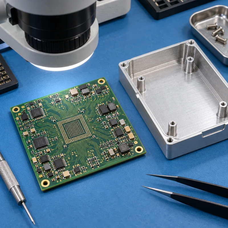
An HDI PCB uses high-density interconnect construction, including microvias and fine routing features, to connect components where conventional routing becomes difficult. It is not defined solely by having many layers. A useful design review connects the electrical stackup to fabrication capability and then checks the assembled board against the enclosure.

This guide addresses engineering handoffs. It does not imply that MTSPi fabricates PCBs or provides a particular electronic assembly certification. Confirm electronic fabrication requirements with the chosen board manufacturer and mechanical component requirements with the machining supplier.

Establish Whether HDI Solves a Real Routing Constraint

Start with the component package, pin map, board outline, routing density, and electrical requirements. A fine-pitch BGA may need a different escape strategy from a larger package with the same logical function. Moving a connector or increasing the board outline may sometimes avoid a costly construction, but those decisions affect the product enclosure and assembly.

Ask the layout engineer to identify the actual bottleneck: insufficient escape channels, excessive layer transitions, limited routing area, or a package geometry that the current via pattern cannot accommodate. “Make it HDI” is not a complete design instruction.

Read the Via Map Alongside the Stackup

Feature Basic role Question to settle
Through via Connects through the board thickness Where does its occupied area restrict routing?
Blind via Connects an outer layer to an internal layer Which layer pair is connected?
Buried via Connects internal layers without reaching an outer surface How is it incorporated into the manufacturing sequence?
Microvia Provides a small, shallow interlayer connection What geometry, filling, and reliability requirements apply?

Do not treat every blind via as a microvia. Supply a layer-pair drawing and define the intended structure. Staggered microvias use offset positions between successive connections; stacked microvias align vertically. They are not interchangeable layout shortcuts. Discuss the specific construction, process capability, and qualification evidence with the fabricator.

Industry HDI design guidance, including Altium’s manufacturing guide, emphasizes that the via structure and manufacturing sequence belong in the design discussion. A visually complete CAD layout does not by itself establish that a shop can manufacture and inspect the intended interconnect reliably.

Select a Manufacturable Build-Up Before Detailed Routing

A notation such as 1+N+1 generally describes one build-up layer on each side of an N-layer core structure. It is a shorthand, not a complete procurement specification. Copper weights, dielectric materials and thicknesses, layer functions, via connections, finished thickness, and impedance requirements still need definition.

Eurocircuits’ published HDI guidance illustrates an important approach: begin with an available build-up and its design rules. Its partial-HDI examples also show that fine routing can be concentrated in part of a construction rather than assumed to require the most complex stack everywhere. Those are supplier-specific offerings, not universal dimensions to copy into an unrelated purchase order.

Agree impedance targets with the actual material and layer structure. Track width alone is insufficient: reference-plane spacing, dielectric properties, copper thickness, and differential-pair spacing all contribute. The board fabricator’s stackup proposal and the designer’s electrical constraints must refer to the same revision.

Check the Mechanical Envelope in Three Dimensions

A smaller board is not automatically a smaller finished product. Connectors, cable bends, component height, thermal hardware, fastening access, and assembly order may control the envelope. A dense board can fit its outline perfectly and still interfere with the enclosure lid.

  • Define a common coordinate origin and mounting-hole datums.
  • Check maximum component height on both sides of the PCB.
  • Include connector mating travel and cable exit space.
  • Keep fasteners and standoffs clear of copper and components as required by the electrical design.
  • Review thermal-pad contact without bending the board through excessive compression.
  • Check access for assembly tools and any required rework.

For an illustrative fit study, export the populated board into the mechanical assembly, add the intended screw heads, and sweep the connector’s mating motion. This can expose a conflict that a bare-board outline check misses. Measure the critical physical interface on first articles instead of relying only on nominal CAD alignment.

Programs using flexible interconnects should also review bend-zone and enclosure-fit considerations. These are separate mechanical constraints, not benefits automatically provided by HDI construction.

Prepare Two Coordinated Manufacturing Packages

The PCB package should contain the agreed fabrication data, layer map, drill and via definitions, stackup, material requirements, finish, impedance targets where applicable, and inspection or test requirements. The mechanical package should contain the enclosure model, drawing, datums, finish, mounting geometry, and approved board envelope.

Use a release table linking both packages to the same assembly revision. If the board thickness changes after quotation, notify the mechanical team: connector height or a retaining feature may depend on that value. Likewise, an enclosure standoff change should not be implemented without checking the populated board.

Discuss machined housing features with MTSPi using the board envelope and interface drawing. Use the project contact page to confirm mechanical scope and required evidence.

Compare Supplier Proposals on Evidence

Request explicit confirmation of the proposed via construction and any departures from the submitted stackup. Compare inspection, electrical testing, documentation, change control, and lot identification rather than accepting “HDI capable” as the complete answer. Acceptance standards and their applicable editions should be agreed in the purchase specification.

Keep electrical continuity, structural reliability, and assembly fit as separate verification questions. A board that passes one check has not necessarily passed the other two.

Frequently Asked Questions

Is every multilayer PCB an HDI board?

No. Layer count alone does not establish HDI construction. Interconnect technology and routing requirements matter.

Can I select microvia sizes after routing?

That risks significant rework. Select the fabricator’s supported stackup and rules before detailed routing.

Does HDI guarantee better signal integrity?

No. Layout, reference planes, materials, transitions, and manufacturing tolerances still require electrical analysis.

Why involve the enclosure supplier early?

The mounting interfaces, component heights, connector positions, and thermal contacts must work together in the finished assembly.

Technical reference basis: Eurocircuits HDI build-up and design guidance; Altium HDI PCB Design and Manufacturing Guide. Mechanical handoff examples are illustrative, not reported customer projects.
Categories
Blog Design, Cost & Sourcing Guides Industries & Applications

Rigid-Flex PCB Design Guide: Stackup, Bend Rules, Enclosures, and Assembly

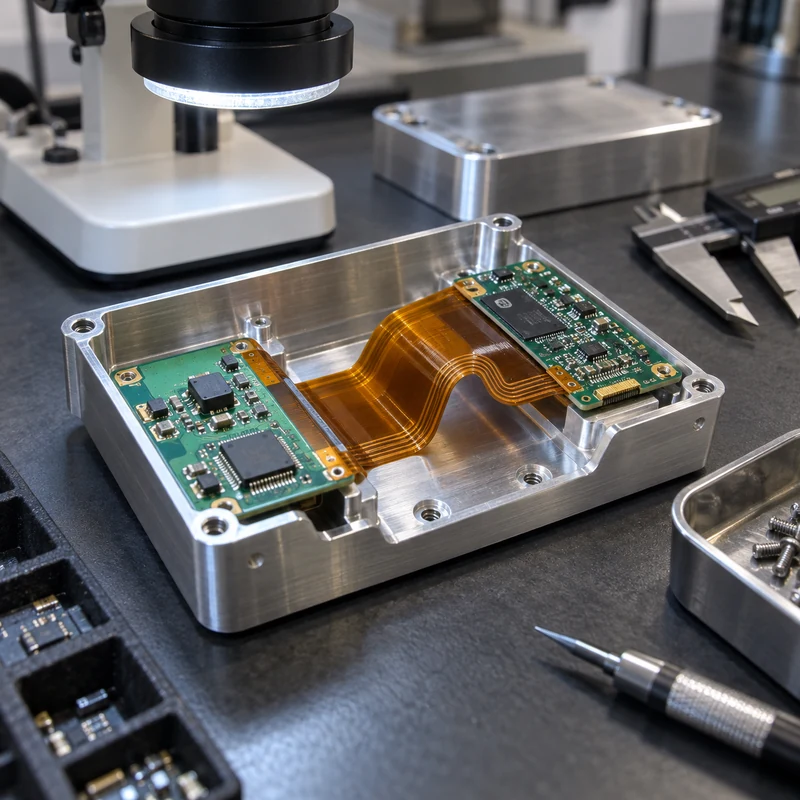
A rigid-flex PCB combines rigid circuit sections with flexible polyimide interconnects in one laminated assembly. It can replace connectors and wire harnesses, save space, reduce assembly steps, and support controlled three-dimensional packaging.

The advantages come with stricter mechanical rules. Bend radius, copper direction, coverlay, layer transitions, stiffeners, enclosure clearances, and assembly sequence must be coordinated early.

Quick Answer

Use rigid-flex when packaging, reliability, weight, or connector reduction justifies the added design and fabrication complexity. Keep bends away from rigid transitions, vias, solder joints, and sharp enclosure edges. Validate the folded state with production-intent stackup and housing geometry.

Key Engineering Factors

Factor Practical effect Control method
Bend radius Too small a radius strains copper and dielectric Set radius from stackup and flex type
Rigid-flex transition Stress concentrates at the boundary Use controlled transition and strain relief
Copper layout Traces across bend can fatigue Route perpendicular to bend and stagger layers
Enclosure clearance Pinching or rubbing damages flex Model dynamic and assembled envelopes
Assembly sequence Fold order can load components Document fixtures and installation steps

How Rigid-Flex Construction Works

Rigid sections commonly use FR4 while flexible sections use polyimide and rolled or electrodeposited copper. Coverlay protects flex conductors. Adhesives, no-flow prepreg, stiffeners, and plated features are selected around stackup and reliability.

Static vs Dynamic Flexing

A static flex bends during assembly and then remains in position. A dynamic flex moves repeatedly in service and needs larger radii, suitable copper, balanced layers, controlled neutral axis, and fatigue validation.

Bend-Area Design Rules

Keep pads, vias, component terminations, abrupt width changes, and rigid edges away from active bends. Curved trace transitions and staggered conductors reduce stress concentration.

  • Route traces perpendicular to bend axis
  • Avoid copper corners and teardrop discontinuities in flex zones
  • Use hatched planes when solid copper makes the section too stiff
  • Define bend direction and final folded angle
  • Confirm minimum radius with the fabricator

Mechanical Enclosure Integration

The housing must support rigid boards while allowing the flex to follow a natural curve. Avoid sharp machined edges, screw interference, compression, and excessive free length. Include assembly access and serviceability.

  • Import the PCB STEP model into enclosure CAD
  • Model the flex in its assembled state
  • Add edge radii and protective clearances
  • Support heavy connectors on rigid sections
  • Check thermal and EMI contact intentionally

Stackup and Fabrication Communication

Provide the controlled stackup, impedance needs, copper weights, materials, surface finish, stiffeners, coverlay openings, controlled-depth features, and test requirements. Ask the fabricator to review the design before layout release.

Assembly and Inspection

Rigid-flex assemblies may require dedicated carriers, fold fixtures, and handling instructions. Inspect conductor continuity, finished outline, plating, coverlay registration, impedance, solder quality, and the final folded assembly.

CNC-Machined Housing Considerations

CNC housings provide strong mounting, shielding, sealing, and thermal paths. Tolerance stacks must include board outline, connector position, standoff height, coating, gasket compression, and flex clearance.

Frequently Asked Questions

How many times can a rigid-flex PCB bend?

Static designs may only bend during assembly; dynamic life depends on stackup, radius, copper, stroke, environment, and testing.

Can vias be placed in the bend area?

They should generally be kept outside active bends because plated holes create stiffness and stress concentration.

Why use rigid-flex instead of cables?

It can reduce connectors, assembly labor, space, weight, and potential connection failures when the program justifies the higher fabrication complexity.

Related MTSPi CNC Resources

Categories
Blog Design, Cost & Sourcing Industries & Applications

4-Layer PCB Basics for Product Developers: Stackup, Uses, and Mechanical Design Notes

4-Layer PCB Basics for Product Developers: Stackup, Uses, and Mechanical Design Notes is a practical manufacturing question because the answer affects cost, lead time, material behavior, inspection, and the path from prototype to production. For MTSPi CNC customers, the key is not simply naming a process, but understanding how the process connects with machined parts, fixtures, tolerances, surface requirements, and final assembly.

This guide explains 4-layer PCB from an engineering and purchasing point of view. It is written for product developers, mechanical engineers, sourcing teams, and buyers who need clear decisions rather than generic process descriptions.

Quick Answer

A 4-layer PCB is often chosen when compact routing, EMI behavior, power distribution, or product reliability requires more than a simple two-layer board. Mechanical design should be coordinated with PCB outline, connector location, heat path, and mounting strategy early.

Key Differences at a Glance

Point Option A Option B
Top layer Components and signal routing Connector height and assembly access
Inner layer 1 Ground plane Shielding and reference stability
Inner layer 2 Power plane or signals Thermal and current planning
Bottom layer Signals and secondary components Clearance to housing, screws, and brackets

How the Process Choice Affects Real Parts

A manufacturing method should be selected around the feature that actually controls function. Cosmetic surfaces, hidden support features, threads, bores, sealing faces, heat-transfer areas, and assembly datums do not carry the same risk. When those requirements are mixed together without priority, quotes become inconsistent and production becomes harder to control.

The safest workflow is to define the part requirement first, then match the process. A printed prototype may answer shape questions, a molded sample may answer appearance questions, and a CNC machined sample may answer tolerance, material, and functional questions. Many successful projects use more than one method before the final design is locked.

Design and Manufacturing Considerations

  • Confirm PCB outline, mounting hole diameter, and keepout zones before machining an enclosure.
  • Use realistic clearance around connectors, switches, displays, LEDs, and cable exits.
  • Plan thermal interfaces when power components need contact with a machined heat sink.
  • Avoid placing conductive metal features too close to exposed pads or antenna zones.
  • Ask for updated board files before cutting production fixtures or housings.

Cost, Lead Time, and Risk Factors

Cost is driven by setup, tooling, material, machine time, inspection, finishing, and revision risk. A low unit price is not always the lowest project cost if it creates rework later. For prototypes and low-volume orders, flexibility can be more valuable than a process with a lower theoretical unit cost.

  • Use standard materials and standard feature sizes when they do not weaken the design.
  • Separate critical tolerances from general dimensions so the supplier knows where to focus.
  • Confirm surface finish and cosmetic requirements before production begins.
  • Avoid late changes to mounting holes, connector openings, datum faces, and threaded features.
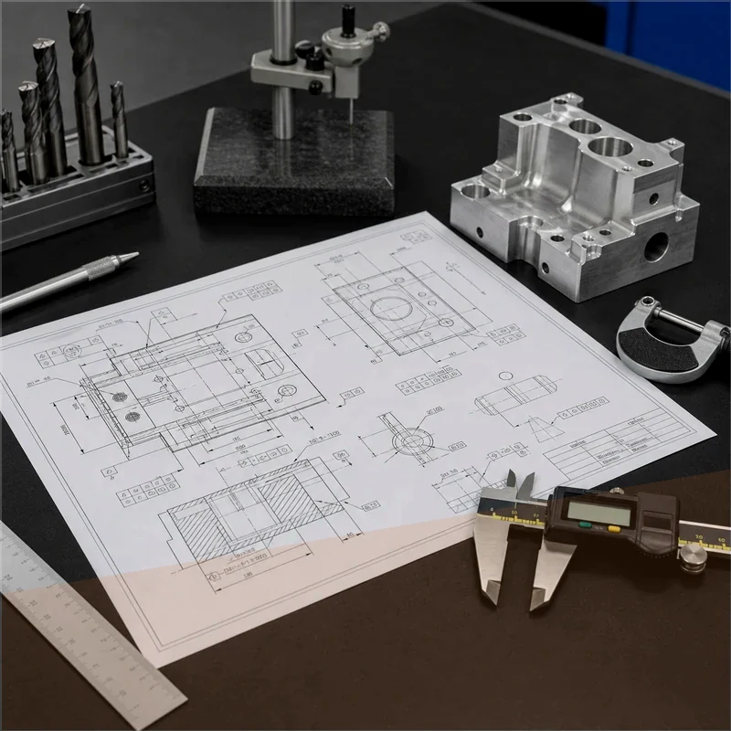
  • Send CAD files and 2D drawings together when tolerances, threads, or finishes matter.

Quality Checks Before Production

A good quality plan checks the features that influence assembly and performance. Depending on the part, this may include dimensional inspection, thread gauges, surface roughness, flatness, perpendicularity, burr control, coating thickness, visual appearance, and fit with mating parts.

When This Topic Matters for CNC Buyers

4-layer PCB matters when a team is comparing prototype routes, validating a design, replacing a weak supplier, or trying to reduce manufacturing cost without damaging function. The best choice is usually the process that answers the current engineering question with the least unnecessary risk.

MTSPi CNC Engineering Notes

MTSPi CNC supports precision CNC milling, turning, rapid prototyping, low-volume production, finishing, and inspection for custom parts. If your project uses molding, casting, welding, PCB assemblies, or 3D printing, CNC machining can still be important for datums, holes, threads, sealing faces, fixtures, and production-ready prototypes.

Frequently Asked Questions

Can this process replace CNC machining?

Sometimes it can replace CNC for non-critical geometry, but CNC is often still needed when tight tolerances, real engineering material, threads, flat sealing faces, or precise mating features are required.

What files help MTSPi CNC review a project?

STEP or STP files are useful for geometry. A 2D drawing is important for tolerances, materials, threads, surface finish, inspection requirements, and notes that are not obvious from the CAD model.

How do I reduce manufacturing risk?

Define critical features, avoid unnecessary tight tolerances, confirm material and finish requirements, and use prototypes to validate assembly before committing to higher-volume tooling or production.

Related MTSPi Resources

Request A Quote

We'll Send You Back with Price Immediately!

DEC 1-31

XMAS SPECEIL

Up to

40% off

4-Layer PCB Basics for Product Developers: Stackup, Uses, and Mechanical Design Notes

We'll Send You Back with Price Immediately!