

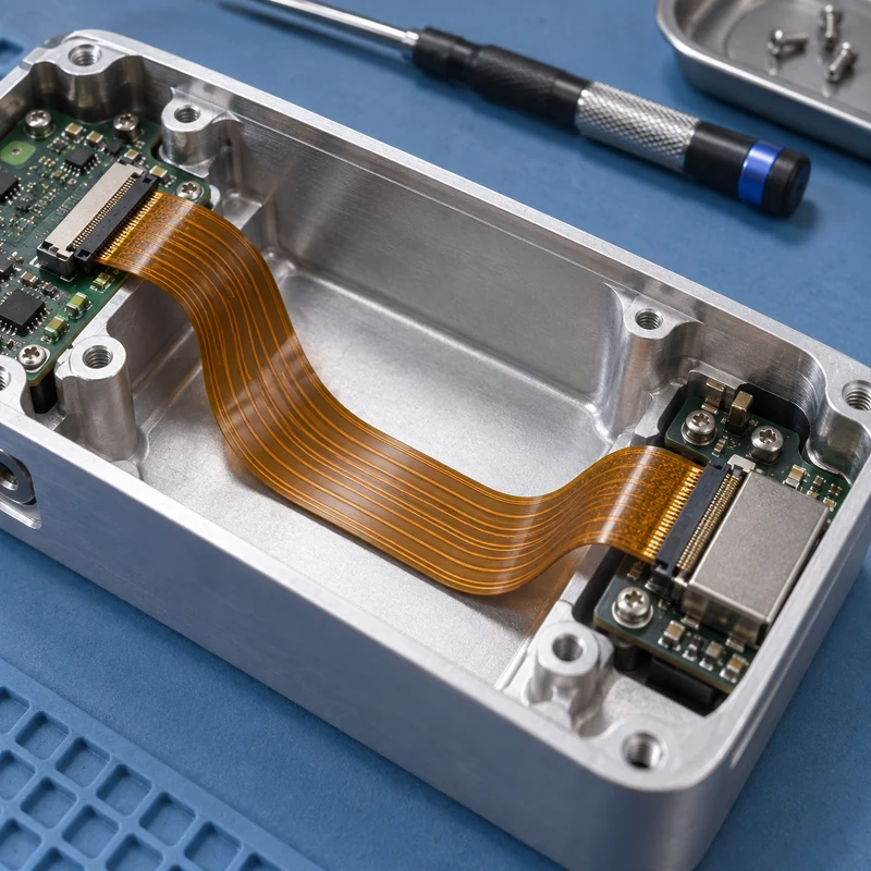
A flexible PCB places conductive tracks on a thin flexible substrate so an electrical connection can follow a three-dimensional route. Successful flexible PCB design combines electrical requirements with mechanical packaging: a circuit that passes a bench continuity test can still be damaged by a connector, enclosure edge, screw, or repeated movement.
Quick answer: Define the installed route and motion first. Agree the stackup, bend radius, bend zones, stiffeners, and connector interfaces with the circuit manufacturer, then verify the assembled product. Treat the flex circuit and its enclosure as interacting parts throughout the design review.
Choose the Circuit Construction Around Its Job
| Construction | Why consider it | Design question |
|---|---|---|
| Single-layer flex | Simple interconnections with a thin flexible region | Can the routing fit without adding layers? |
| Double-sided or multilayer flex | More routing density and electrical functions | Does the complete stack remain suitable for the required bend? |
| Flex with local stiffeners | Supported connectors or component areas | Where does the stiffener end relative to the bend? |
| Rigid-flex assembly | Integrated rigid component regions and flexible connections | Does integration justify the fabrication and assembly complexity? |
Rigid-flex is a distinct construction rather than simply a flexible board with a reinforcing patch. For that option, review the rigid-flex stackup and assembly guide alongside the housing design.
Separate Installation Bends From Repeated Movement
A circuit formed once during installation has a different duty from one moving through thousands of cycles. Vibration or service access can add movement even when the product appears static. Define the movement, expected cycles, temperature, and assembly handling before asking for a minimum radius.
The complete flexible-region thickness includes the copper, dielectric, adhesive where present, and protective layers. Material construction and copper type also affect bending behavior. Obtain a radius recommendation for the actual stackup and duty, rather than applying a universal multiplier to every design.
Make Material Choices With the Fabricator
Polyimide is a common flexible-circuit substrate. Copper construction, coverlay, adhesives, and stiffeners must be selected as a system. Rolled-annealed copper is often considered where flexing performance is important; material selection still needs confirmation for the intended use.
Publish the approved stackup and material requirements with the fabrication data. A part-number change affecting thickness can alter the mechanical fit even if the electrical connectivity remains unchanged. Include the mechanical owner in changes that affect the flexible region or connector thickness.
Reserve Bend Zones in the Layout
Identify bend regions explicitly and coordinate trace routing, vias, components, and stiffener boundaries around them. Avoid forcing the circuit to bend at a sudden rigid transition. Ask the manufacturer to review the combination of routing and mechanical constraints before releasing the files.
A convenient approach is to include both a flat circuit outline and the installed shape in the design package. The flat view defines manufacturing geometry; the installed view communicates where the circuit travels and what occupies the surrounding space. Keep their revision identifiers synchronized.
Design the Enclosure Around the Installed Circuit
Model the circuit’s occupied volume rather than a zero-thickness line. Include the bend, adjacent components, connector access, and the space needed during installation. Provide an intentional route that does not depend on an assembler pressing the loop into an arbitrary corner.
- Keep the circuit clear of screw tips and closing cover edges.
- Remove burrs and review edges where contact is possible.
- Provide access to operate the connector latch.
- Allow installation without pulling on the conductor region.
- Check the circuit position with the cover fully closed.
For a machined housing, discuss those details with the CNC milling team. Rounded features, suitable surface treatment, and accessible assembly geometry belong on the controlled housing drawing.
Use a Clearance Budget Instead of a Visual Guess
Consider an illustrative assembly with a nominal 1.5 mm gap between a flex loop and a cover. If housing variation, circuit positioning, and installation variation can each consume 0.3 mm in the unfavorable direction, the simple worst-case remaining gap is 0.6 mm. This example is not a recommended clearance; it demonstrates why nominal CAD separation alone is insufficient.
Add the actual tolerances and motion from your product. Check whether the assembly has a defined locating feature or whether the circuit can wander. When position is uncontrolled, improving the route or retention can be more effective than tightening a machining tolerance.
Prototype the Assembly Sequence
Build a fit model early enough to move the connector or change the housing. Record how the circuit is inserted, latched, formed, inspected, and serviced. A design that fits after difficult manipulation can still fail in repeat production.
Use prototype enclosures and fixtures to evaluate access and routing. Use representative circuit materials for decisions about bending; a paper mock-up can demonstrate route length but cannot validate the mechanical life of the final circuit.
Verify the Complete Product
Electrical testing of the bare circuit and testing of the assembled product answer different questions. Define checks for continuity, shorts, connector engagement, and damage after assembly. Where repeated flexing is part of the duty, agree a representative test with the responsible electronics and reliability engineers.
Photograph the approved routing position for assembly instructions. Record the circuit revision, enclosure revision, connector, and any adhesive or retention method. When a failure occurs, inspect the actual contact point and bend location rather than assuming the board material is the only cause.
Frequently Asked Questions
Can a flexible PCB be folded sharply?
Do not assume it can. The allowable bend depends on the stackup and duty. A sharp crease can damage conductors even if the circuit initially passes an electrical check.
Is the thinnest circuit always best?
No. Electrical, thermal, handling, connector, and fabrication requirements also apply. Choose an approved construction that meets the combined requirements.
Does a prototype housing prove flex life?
No. It can reveal access and clearance problems. Flex life requires suitable testing of representative materials, routing, and operating conditions.