

Categories
Blog Design, Cost & Sourcing

Flexible PCB Design: Bend Zones, Materials, and Enclosure Fit

A flexible PCB places conductive tracks on a thin flexible substrate so an electrical connection can follow a three-dimensional route. Successful flexible PCB design combines electrical requirements with mechanical packaging: a circuit that passes a bench continuity test can still be damaged by a connector, enclosure edge, screw, or repeated movement.

Quick answer: Define the installed route and motion first. Agree the stackup, bend radius, bend zones, stiffeners, and connector interfaces with the circuit manufacturer, then verify the assembled product. Treat the flex circuit and its enclosure as interacting parts throughout the design review.

Choose the Circuit Construction Around Its Job

Construction Why consider it Design question
Single-layer flex Simple interconnections with a thin flexible region Can the routing fit without adding layers?
Double-sided or multilayer flex More routing density and electrical functions Does the complete stack remain suitable for the required bend?
Flex with local stiffeners Supported connectors or component areas Where does the stiffener end relative to the bend?
Rigid-flex assembly Integrated rigid component regions and flexible connections Does integration justify the fabrication and assembly complexity?

Rigid-flex is a distinct construction rather than simply a flexible board with a reinforcing patch. For that option, review the rigid-flex stackup and assembly guide alongside the housing design.

Separate Installation Bends From Repeated Movement

A circuit formed once during installation has a different duty from one moving through thousands of cycles. Vibration or service access can add movement even when the product appears static. Define the movement, expected cycles, temperature, and assembly handling before asking for a minimum radius.

The complete flexible-region thickness includes the copper, dielectric, adhesive where present, and protective layers. Material construction and copper type also affect bending behavior. Obtain a radius recommendation for the actual stackup and duty, rather than applying a universal multiplier to every design.

Make Material Choices With the Fabricator

Polyimide is a common flexible-circuit substrate. Copper construction, coverlay, adhesives, and stiffeners must be selected as a system. Rolled-annealed copper is often considered where flexing performance is important; material selection still needs confirmation for the intended use.

Publish the approved stackup and material requirements with the fabrication data. A part-number change affecting thickness can alter the mechanical fit even if the electrical connectivity remains unchanged. Include the mechanical owner in changes that affect the flexible region or connector thickness.

Reserve Bend Zones in the Layout

Identify bend regions explicitly and coordinate trace routing, vias, components, and stiffener boundaries around them. Avoid forcing the circuit to bend at a sudden rigid transition. Ask the manufacturer to review the combination of routing and mechanical constraints before releasing the files.

A convenient approach is to include both a flat circuit outline and the installed shape in the design package. The flat view defines manufacturing geometry; the installed view communicates where the circuit travels and what occupies the surrounding space. Keep their revision identifiers synchronized.

Design the Enclosure Around the Installed Circuit

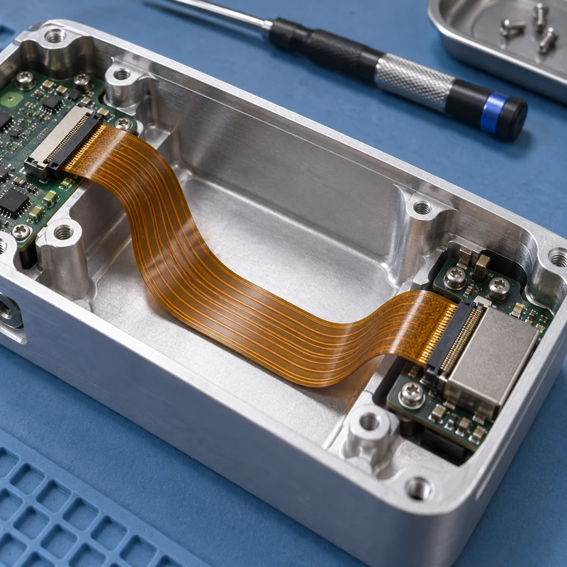
Model the circuit’s occupied volume rather than a zero-thickness line. Include the bend, adjacent components, connector access, and the space needed during installation. Provide an intentional route that does not depend on an assembler pressing the loop into an arbitrary corner.

  • Keep the circuit clear of screw tips and closing cover edges.
  • Remove burrs and review edges where contact is possible.
  • Provide access to operate the connector latch.
  • Allow installation without pulling on the conductor region.
  • Check the circuit position with the cover fully closed.

For a machined housing, discuss those details with the CNC milling team. Rounded features, suitable surface treatment, and accessible assembly geometry belong on the controlled housing drawing.

Use a Clearance Budget Instead of a Visual Guess

Consider an illustrative assembly with a nominal 1.5 mm gap between a flex loop and a cover. If housing variation, circuit positioning, and installation variation can each consume 0.3 mm in the unfavorable direction, the simple worst-case remaining gap is 0.6 mm. This example is not a recommended clearance; it demonstrates why nominal CAD separation alone is insufficient.

Add the actual tolerances and motion from your product. Check whether the assembly has a defined locating feature or whether the circuit can wander. When position is uncontrolled, improving the route or retention can be more effective than tightening a machining tolerance.

Prototype the Assembly Sequence

Build a fit model early enough to move the connector or change the housing. Record how the circuit is inserted, latched, formed, inspected, and serviced. A design that fits after difficult manipulation can still fail in repeat production.

Use prototype enclosures and fixtures to evaluate access and routing. Use representative circuit materials for decisions about bending; a paper mock-up can demonstrate route length but cannot validate the mechanical life of the final circuit.

Verify the Complete Product

Electrical testing of the bare circuit and testing of the assembled product answer different questions. Define checks for continuity, shorts, connector engagement, and damage after assembly. Where repeated flexing is part of the duty, agree a representative test with the responsible electronics and reliability engineers.

Photograph the approved routing position for assembly instructions. Record the circuit revision, enclosure revision, connector, and any adhesive or retention method. When a failure occurs, inspect the actual contact point and bend location rather than assuming the board material is the only cause.

Frequently Asked Questions

Can a flexible PCB be folded sharply?

Do not assume it can. The allowable bend depends on the stackup and duty. A sharp crease can damage conductors even if the circuit initially passes an electrical check.

Is the thinnest circuit always best?

No. Electrical, thermal, handling, connector, and fabrication requirements also apply. Choose an approved construction that meets the combined requirements.

Does a prototype housing prove flex life?

No. It can reveal access and clearance problems. Flex life requires suitable testing of representative materials, routing, and operating conditions.
Categories
Blog Design, Cost & Sourcing Guides Industries & Applications

Rigid-Flex PCB Design Guide: Stackup, Bend Rules, Enclosures, and Assembly

A rigid-flex PCB combines rigid circuit sections with flexible polyimide interconnects in one laminated assembly. It can replace connectors and wire harnesses, save space, reduce assembly steps, and support controlled three-dimensional packaging.

The advantages come with stricter mechanical rules. Bend radius, copper direction, coverlay, layer transitions, stiffeners, enclosure clearances, and assembly sequence must be coordinated early.

Quick Answer

Use rigid-flex when packaging, reliability, weight, or connector reduction justifies the added design and fabrication complexity. Keep bends away from rigid transitions, vias, solder joints, and sharp enclosure edges. Validate the folded state with production-intent stackup and housing geometry.

Key Engineering Factors

Factor Practical effect Control method
Bend radius Too small a radius strains copper and dielectric Set radius from stackup and flex type
Rigid-flex transition Stress concentrates at the boundary Use controlled transition and strain relief
Copper layout Traces across bend can fatigue Route perpendicular to bend and stagger layers
Enclosure clearance Pinching or rubbing damages flex Model dynamic and assembled envelopes
Assembly sequence Fold order can load components Document fixtures and installation steps

How Rigid-Flex Construction Works

Rigid sections commonly use FR4 while flexible sections use polyimide and rolled or electrodeposited copper. Coverlay protects flex conductors. Adhesives, no-flow prepreg, stiffeners, and plated features are selected around stackup and reliability.

Static vs Dynamic Flexing

A static flex bends during assembly and then remains in position. A dynamic flex moves repeatedly in service and needs larger radii, suitable copper, balanced layers, controlled neutral axis, and fatigue validation.

Bend-Area Design Rules

Keep pads, vias, component terminations, abrupt width changes, and rigid edges away from active bends. Curved trace transitions and staggered conductors reduce stress concentration.

  • Route traces perpendicular to bend axis
  • Avoid copper corners and teardrop discontinuities in flex zones
  • Use hatched planes when solid copper makes the section too stiff
  • Define bend direction and final folded angle
  • Confirm minimum radius with the fabricator

Mechanical Enclosure Integration

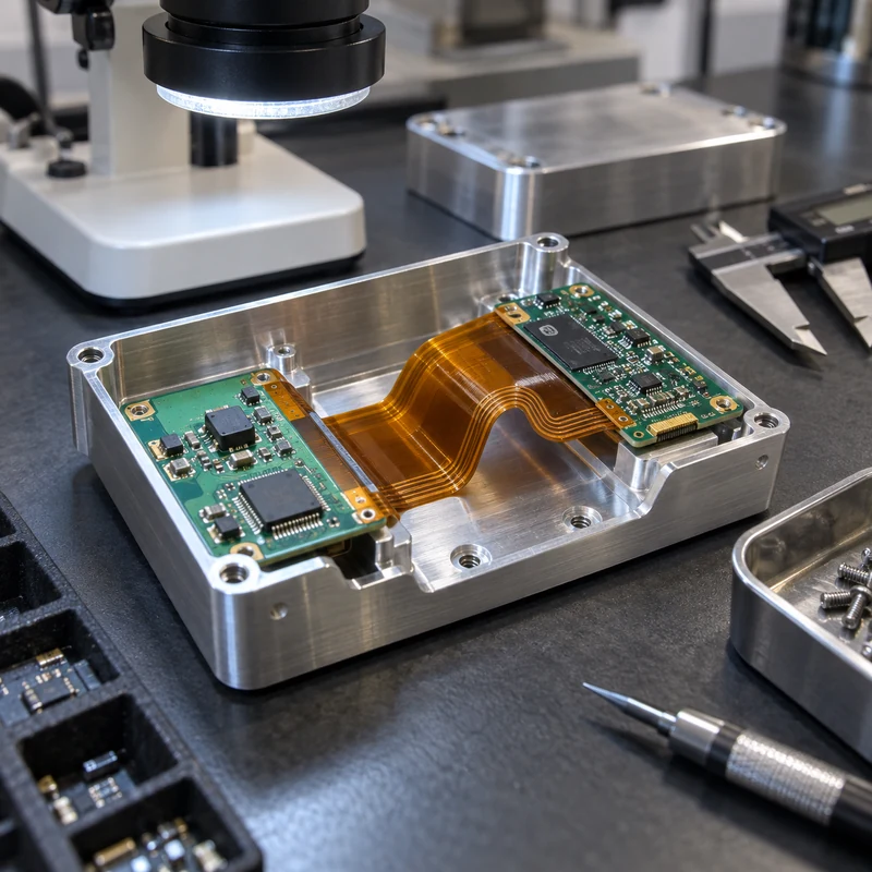
The housing must support rigid boards while allowing the flex to follow a natural curve. Avoid sharp machined edges, screw interference, compression, and excessive free length. Include assembly access and serviceability.

  • Import the PCB STEP model into enclosure CAD
  • Model the flex in its assembled state
  • Add edge radii and protective clearances
  • Support heavy connectors on rigid sections
  • Check thermal and EMI contact intentionally

Stackup and Fabrication Communication

Provide the controlled stackup, impedance needs, copper weights, materials, surface finish, stiffeners, coverlay openings, controlled-depth features, and test requirements. Ask the fabricator to review the design before layout release.

Assembly and Inspection

Rigid-flex assemblies may require dedicated carriers, fold fixtures, and handling instructions. Inspect conductor continuity, finished outline, plating, coverlay registration, impedance, solder quality, and the final folded assembly.

CNC-Machined Housing Considerations

CNC housings provide strong mounting, shielding, sealing, and thermal paths. Tolerance stacks must include board outline, connector position, standoff height, coating, gasket compression, and flex clearance.

Frequently Asked Questions

How many times can a rigid-flex PCB bend?

Static designs may only bend during assembly; dynamic life depends on stackup, radius, copper, stroke, environment, and testing.

Can vias be placed in the bend area?

They should generally be kept outside active bends because plated holes create stiffness and stress concentration.

Why use rigid-flex instead of cables?

It can reduce connectors, assembly labor, space, weight, and potential connection failures when the program justifies the higher fabrication complexity.

Related MTSPi CNC Resources

Categories
Blog Design, Cost & Sourcing Industries & Applications

4-Layer PCB Basics for Product Developers: Stackup, Uses, and Mechanical Design Notes

4-Layer PCB Basics for Product Developers: Stackup, Uses, and Mechanical Design Notes is a practical manufacturing question because the answer affects cost, lead time, material behavior, inspection, and the path from prototype to production. For MTSPi CNC customers, the key is not simply naming a process, but understanding how the process connects with machined parts, fixtures, tolerances, surface requirements, and final assembly.

This guide explains 4-layer PCB from an engineering and purchasing point of view. It is written for product developers, mechanical engineers, sourcing teams, and buyers who need clear decisions rather than generic process descriptions.

Quick Answer

A 4-layer PCB is often chosen when compact routing, EMI behavior, power distribution, or product reliability requires more than a simple two-layer board. Mechanical design should be coordinated with PCB outline, connector location, heat path, and mounting strategy early.

Key Differences at a Glance

Point Option A Option B
Top layer Components and signal routing Connector height and assembly access
Inner layer 1 Ground plane Shielding and reference stability
Inner layer 2 Power plane or signals Thermal and current planning
Bottom layer Signals and secondary components Clearance to housing, screws, and brackets

How the Process Choice Affects Real Parts

A manufacturing method should be selected around the feature that actually controls function. Cosmetic surfaces, hidden support features, threads, bores, sealing faces, heat-transfer areas, and assembly datums do not carry the same risk. When those requirements are mixed together without priority, quotes become inconsistent and production becomes harder to control.

The safest workflow is to define the part requirement first, then match the process. A printed prototype may answer shape questions, a molded sample may answer appearance questions, and a CNC machined sample may answer tolerance, material, and functional questions. Many successful projects use more than one method before the final design is locked.

Design and Manufacturing Considerations

  • Confirm PCB outline, mounting hole diameter, and keepout zones before machining an enclosure.
  • Use realistic clearance around connectors, switches, displays, LEDs, and cable exits.
  • Plan thermal interfaces when power components need contact with a machined heat sink.
  • Avoid placing conductive metal features too close to exposed pads or antenna zones.
  • Ask for updated board files before cutting production fixtures or housings.

Cost, Lead Time, and Risk Factors

Cost is driven by setup, tooling, material, machine time, inspection, finishing, and revision risk. A low unit price is not always the lowest project cost if it creates rework later. For prototypes and low-volume orders, flexibility can be more valuable than a process with a lower theoretical unit cost.

  • Use standard materials and standard feature sizes when they do not weaken the design.
  • Separate critical tolerances from general dimensions so the supplier knows where to focus.
  • Confirm surface finish and cosmetic requirements before production begins.
  • Avoid late changes to mounting holes, connector openings, datum faces, and threaded features.
  • Send CAD files and 2D drawings together when tolerances, threads, or finishes matter.

Quality Checks Before Production

A good quality plan checks the features that influence assembly and performance. Depending on the part, this may include dimensional inspection, thread gauges, surface roughness, flatness, perpendicularity, burr control, coating thickness, visual appearance, and fit with mating parts.

When This Topic Matters for CNC Buyers

4-layer PCB matters when a team is comparing prototype routes, validating a design, replacing a weak supplier, or trying to reduce manufacturing cost without damaging function. The best choice is usually the process that answers the current engineering question with the least unnecessary risk.

MTSPi CNC Engineering Notes

MTSPi CNC supports precision CNC milling, turning, rapid prototyping, low-volume production, finishing, and inspection for custom parts. If your project uses molding, casting, welding, PCB assemblies, or 3D printing, CNC machining can still be important for datums, holes, threads, sealing faces, fixtures, and production-ready prototypes.

Frequently Asked Questions

Can this process replace CNC machining?

Sometimes it can replace CNC for non-critical geometry, but CNC is often still needed when tight tolerances, real engineering material, threads, flat sealing faces, or precise mating features are required.

What files help MTSPi CNC review a project?

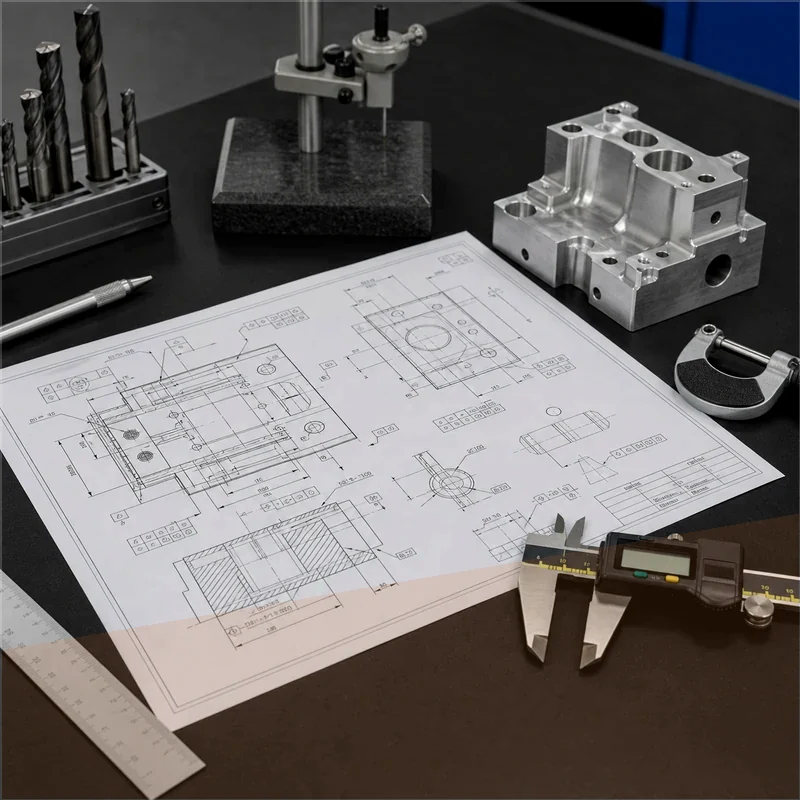
STEP or STP files are useful for geometry. A 2D drawing is important for tolerances, materials, threads, surface finish, inspection requirements, and notes that are not obvious from the CAD model.

How do I reduce manufacturing risk?

Define critical features, avoid unnecessary tight tolerances, confirm material and finish requirements, and use prototypes to validate assembly before committing to higher-volume tooling or production.

Related MTSPi Resources

Request A Quote

We'll Send You Back with Price Immediately!

DEC 1-31

XMAS SPECEIL

Up to

40% off

4-Layer PCB Basics for Product Developers: Stackup, Uses, and Mechanical Design Notes

We'll Send You Back with Price Immediately!